LPDDR5 Tutorial: Deep dive into its physical structure
Introduction
In this article, we'll take a detailed look at the physical structure of LPDDR5 memory, starting from the basics and working our way up. By the end, you'll have a clear understanding of key terms related to LPDDR5 memory, including:
- LPDDR5 IOs: Command Bus (CA), Data Bus (DQ/DQS), ChipSelect (CS), Clock (CK)
- Bank and Bank Group Architecture
- Ranks and Page Size
- LPDDR5 Memory Channels
- Interpretation of x16/x32/x64 widths
We'll begin with a single DRAM memory cell and gradually explore how it forms a complete Memory Package soldered onto a PCB.
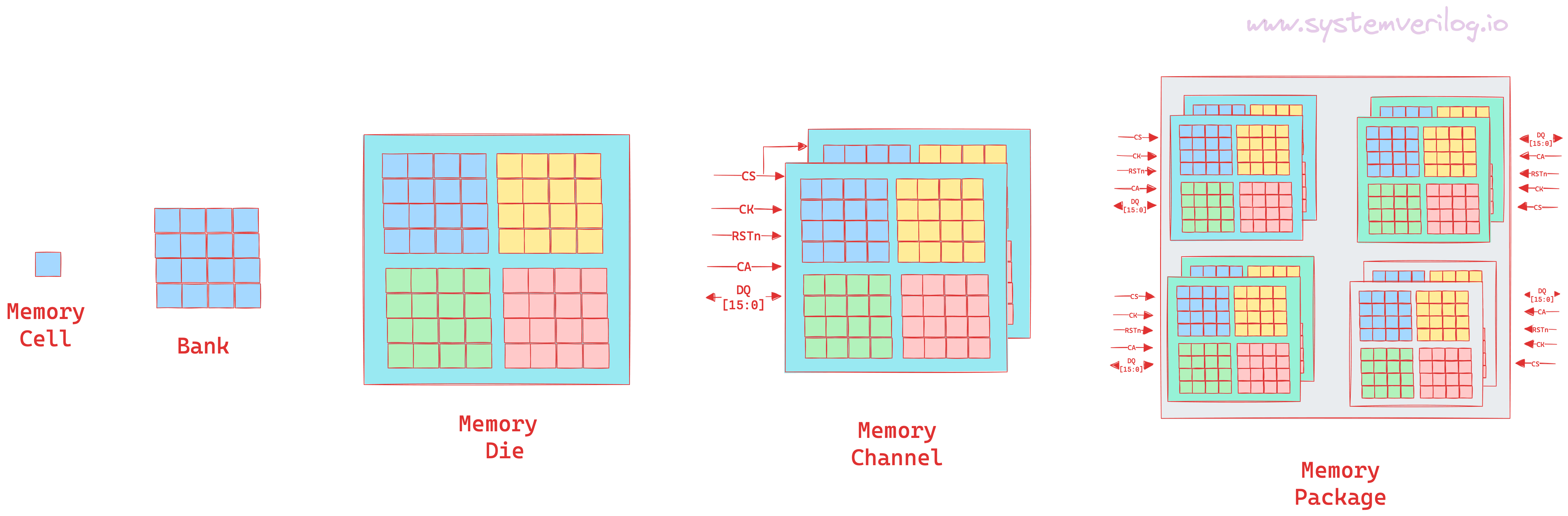
The LPDDR5 Memory Die
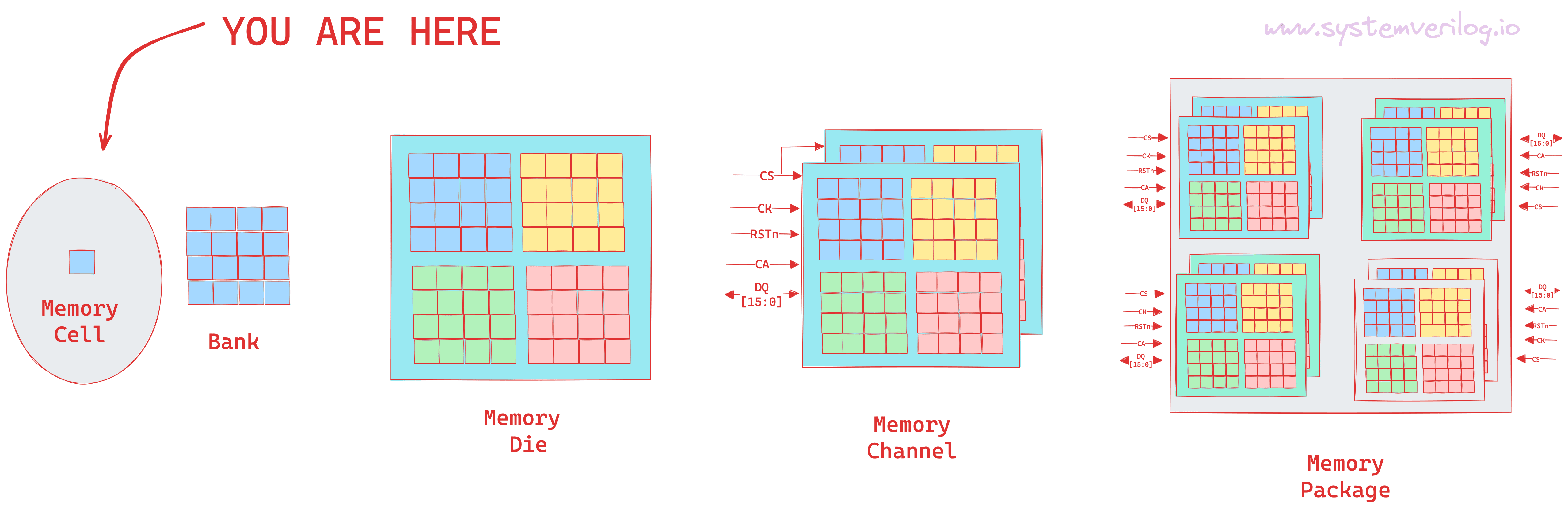
A Single Memory Cell
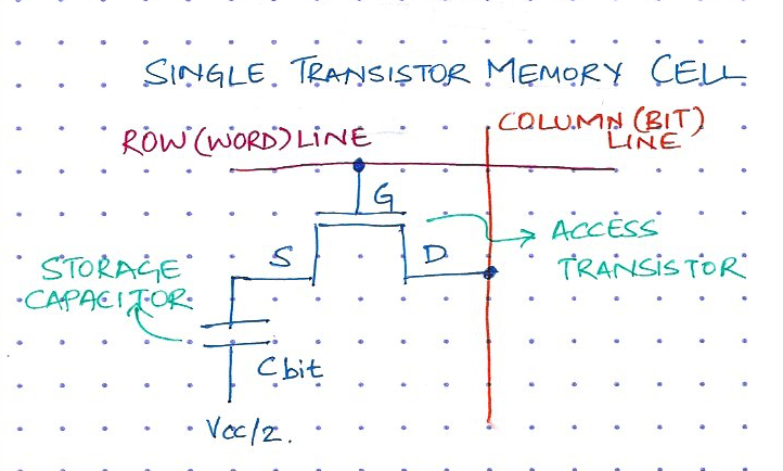
At the lowest level, a bit is essentially a capacitor that holds the charge and a transistor acting as a switch. Since the capacitor discharges over time, the information eventually fades unless the capacitor is periodically REFRESHed. This is where the D in DRAM comes from - it refers to Dynamic as opposed to the Static in SRAM.
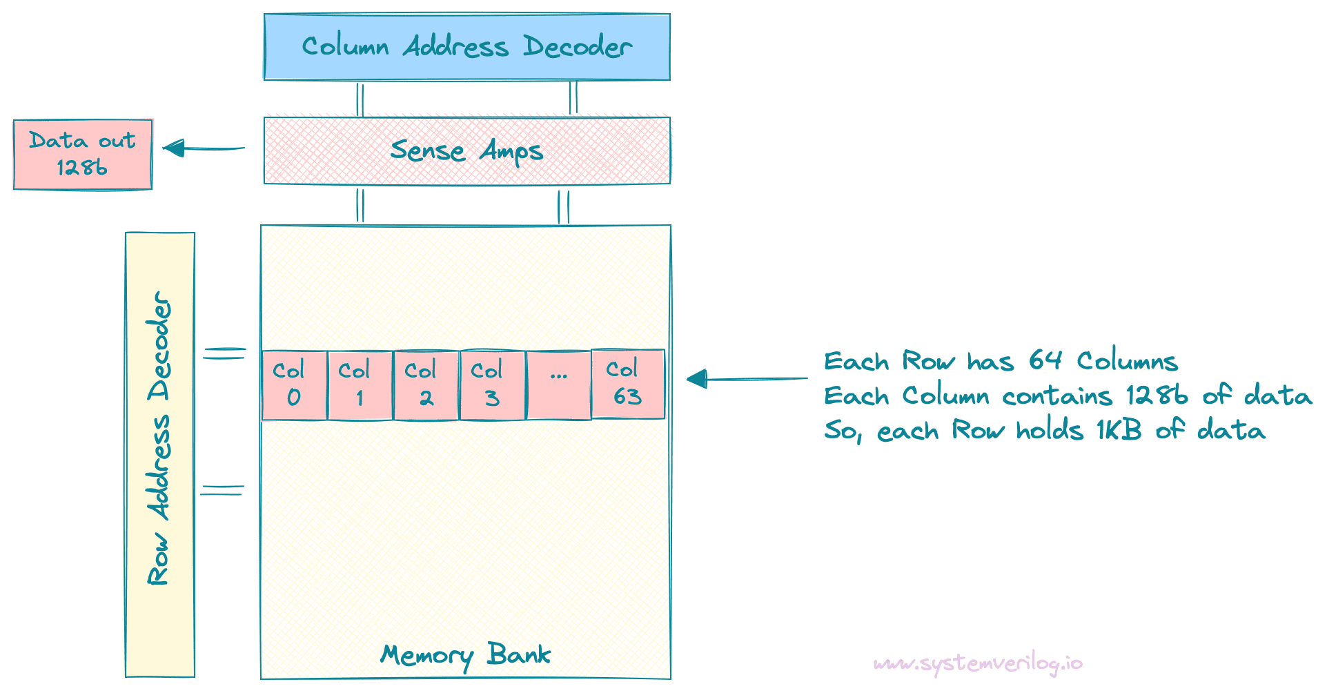
Bank, Rows and Columns
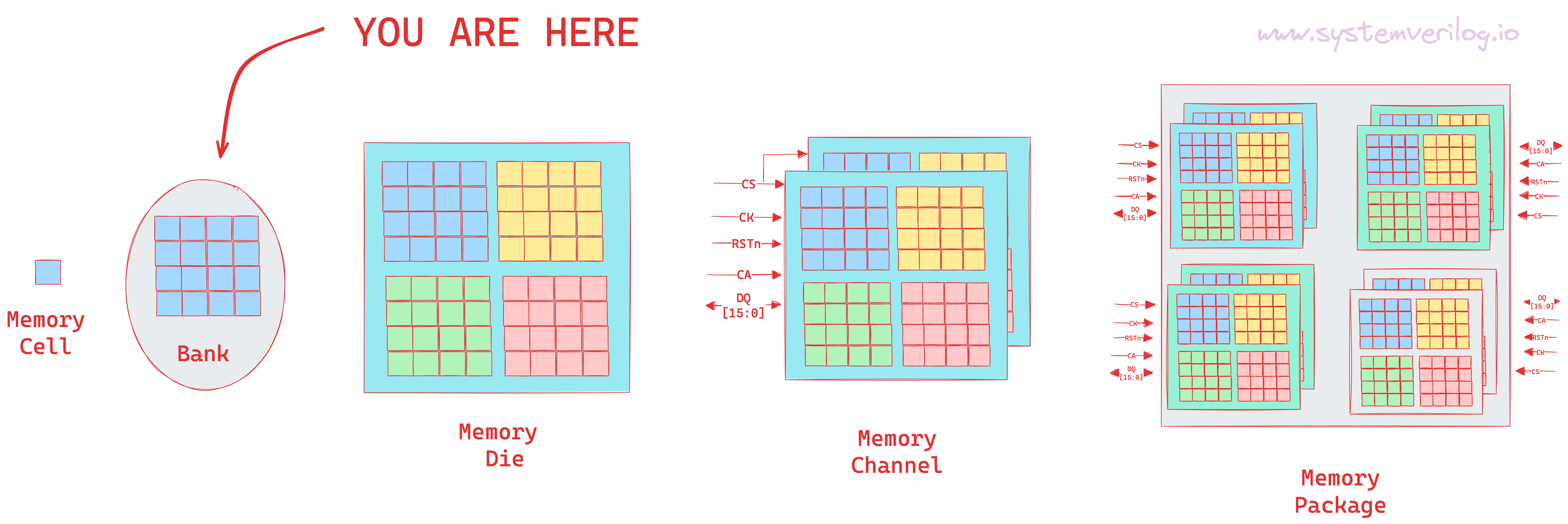
When you zoom out one level, you will notice Memory Cells arranged in a grid of Rows and Columns.
One such grid of memory cells is called a Bank. A Bank also has a structure called Sense Amps. During a READ operation, a Row is first ACTIVATED and loaded into the Sense Amps. The Column address is then used to read out the appropriate column bits.
In LPDDR5,
- Each Row of a Bank holds 1KB (8192 bits) of data
- This 1KB in each row is arranged into 64 Columns of 128b each.
[64 x 128b = 8192b] - So, with each
READ/WRITEaccess a Row Address and a Column address is specified and the bank returns 128b of data. This number is important, we'll revisit it once again in the next section.
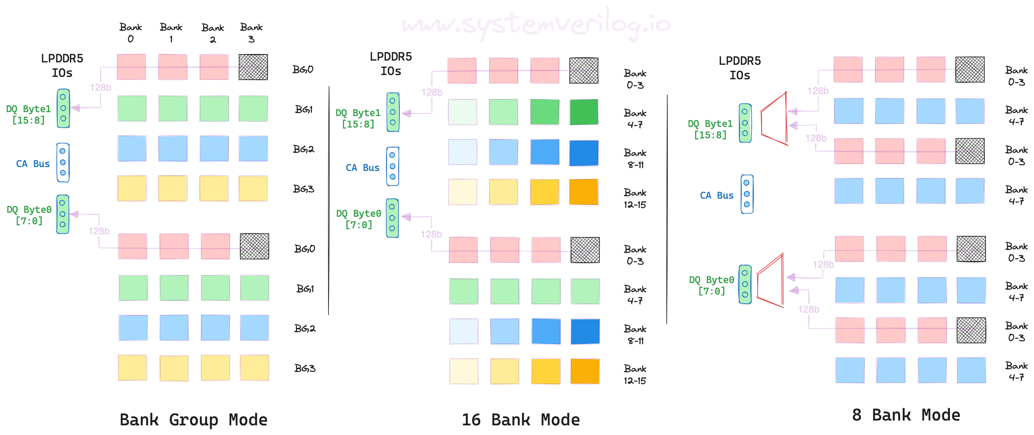
LPDDR5 Bank Architecture
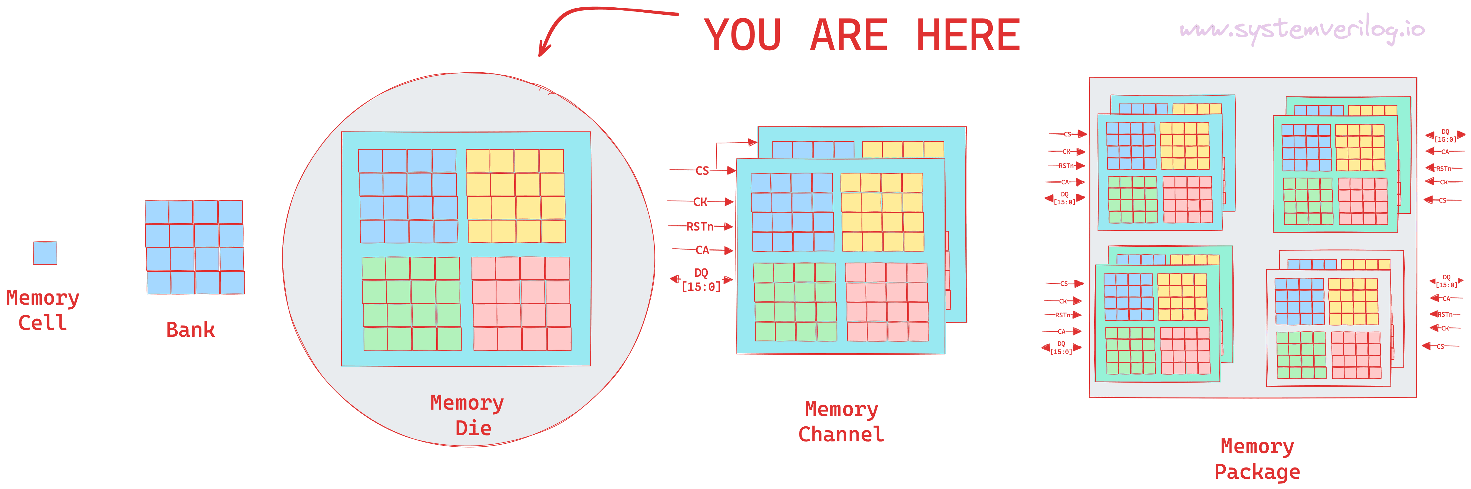
Zooming out another level, each LPDDR5 Die has 32 of these Bank tile. These 32 tiles can be arranged in 3 different configurations.
Bank Group Mode- Also known as BG Mode. Here the 32 Bank tiles are organized into 2 sets of 4 Bank Groups with 4 Banks each.
[2x4x4 = 32]. - In Figure 3 below, notice the
BG0,1,2,3along Y-axis andBank0,1,2,3along X. - During a
READ/WRITEoperation, the supplied bank address activates 2 banks and a total of 256b is accessed (Remember, each Row and Col address access 128b within a bank).
- Also known as BG Mode. Here the 32 Bank tiles are organized into 2 sets of 4 Bank Groups with 4 Banks each.
16 Bank Mode- In this mode the 32 Bank tiles are organized into 2 sets of 16 Banks
[2 x 16 = 32]. - The difference between this mode and the Bank Group Mode is that, the timing parameters to access the banks are different between the two modes. As you will see later, the 16 Bank Mode can only operate at speeds below 3200 Mbps whereas BG Mode operates at speeds greater than 3200 Mbps.
- In this mode the 32 Bank tiles are organized into 2 sets of 16 Banks
8 Bank Mode- Here the 32 Bank tiles are organized into 4 sets of 8 Banks
[4 x 8 = 32]. So, during aREAD/WRITEoperation, the supplied bank address activates 4 banks and a total of 512b is accessed.
- Here the 32 Bank tiles are organized into 4 sets of 8 Banks
Why are there 3 Bank Modes and not just one? 🤔
LPDDR5 offers multiple Bank Modes to accomodate different speeds of operation (such as 3200Mbps, 5400Mbps, 6400 Mbps, etc.) and different data access widths (256b and 512b). Bank Mode selection is done during initialization by setting a parameter in Mode Register MR3 (The default setting is 16B Mode).
So, which among the 3 configurations you choose depends on 2 factors
Speed Grade- What speed is the memory is operating at?Native Burst Length- How many bits of data do you want to read/write with each operation?
Let us look at these in detail.
Speed Grade
- Bank Group Mode can only be used if the memory is operating > 3200Mb/s
- 16 Bank Mode can only be used if the memory is operating <= 3200Mb/s
- 8 Bank Mode can be accessed at all speeds
Native Burst Length
- In 16 Bank Mode and Bank Group Mode, a Read operation activates 2 Banks in parallel and accesses 256b of data (Remember each Bank returns 128b). In LPDDR5, the Data Bus is 16 bits wide (
DQ[15:0]). So the 256b of data is then streamed out in a burst of 16 chunks, with each chunk being 16b (16x16 = 256). This is also called BL16 or Burst Length 16. - In 8 Bank Mode, as you see in Figure 3, each READ/WRITE operation activates 4 banks and a total of 512b of data is fetched. This data is then streamed out in a burst of 32 beats with each beat holding 16b of data (32x16 = 512). This is called Burst Length 32.
Example: If your system is designed to operate at 6400Mb/s (the highest speed LPDDR5 supports), and you require data access at 256b granularity, then you would choose the Bank Group Mode.
Note
You can do BL32 in Bank Group mode too, but its a bit more complex and does some interleaving of data. You are better off just using 8B Mode if you want a Burst Length of 32.
Page Size
Page Size is the number of bits loaded into the Sense Amps when a row is activated.
- In 16 Bank Mode and Bank Group Mode the Page Size is 2KB
- In 8B Mode Page Size is 4KB
How did we arrive at these numbers?
In Figure 2 we saw that each Row in a bank holds 1KB of data (arranged as 64 columns of 128b); and, from Figure 3 in 16 Bank and Bank Group Modes two banks are activated simultaneously to fetch total of 256b. So, from the memory die's point of view, 2 banks are activated and total page size is 2x1KB = 2KB.
Following from that, in case of 8 bank mode one access activates 4 banks hence page size is 4KB.
Density
So far we have discussed the physical structure of a LPDDR5 memory die, but what is the capacity of a memory die, how many bits can it hold?
The LPDDR5 memory die is manufactured in specific capacities, from 2Gb to 32Gb, as specified in the JEDEC Specification. The main difference between a die with 2Gb capacity and that with 32Gb is the number of rows in each bank. The table below shows the number of address bits for a memory operating in BG mode.
| Memory Density | 2Gb | 8Gb | 16Gb | 32Gb |
|---|---|---|---|---|
| Number of Rows | 8192 | 32,768 | 65,536 | 131,072 |
| Number of Cols | 64 | 64 | 64 | 64 |
| Row Address Bits | R0-R12 | R0-R14 | R0-R15 | R0-R16 |
| Col Address Bits | C0-C5 | C0-C5 | C0-C5 | C0-C5 |
| Bank Address Bits | BA0-BA1 | BA0-BA1 | BA0-BA1 | BA0-BA1 |
| BG Address Bits | BG0-BG1 | BA0-BA1 | BA0-BA1 | BA0-BA1 |
| Page Size | 2KB | 2KB | 2KB | 2KB |
| Array Pre-Fetch | 256b | 256b | 256b | 256b |
Arriving at the total density of a 2Gb die:
 4 (BG) x 4 (Banks) x 8192 (rows) x 64 (cols) x 256b (each col) = 2,147,483,648 = 2Gb
Putting it all together
Analogy Time
A DRAM chip is equivalent to a building full of file cabinets
Bank GroupIdentifies the floor number
Bank AddressIdentifies the file cabinet within that floor where the file you need is located
Row AddressIdentifies which drawer in the cabinet the file is located. Reading data into the Sense Amplifiers is equivalent to opening/pulling out the file drawer.
Col AddressIdentifies the file number within this drawer. When you want to read another row, you have to put this file back in the drawer and close it before opening the next drawer. This is equivalent toPRECHARGE-ing.
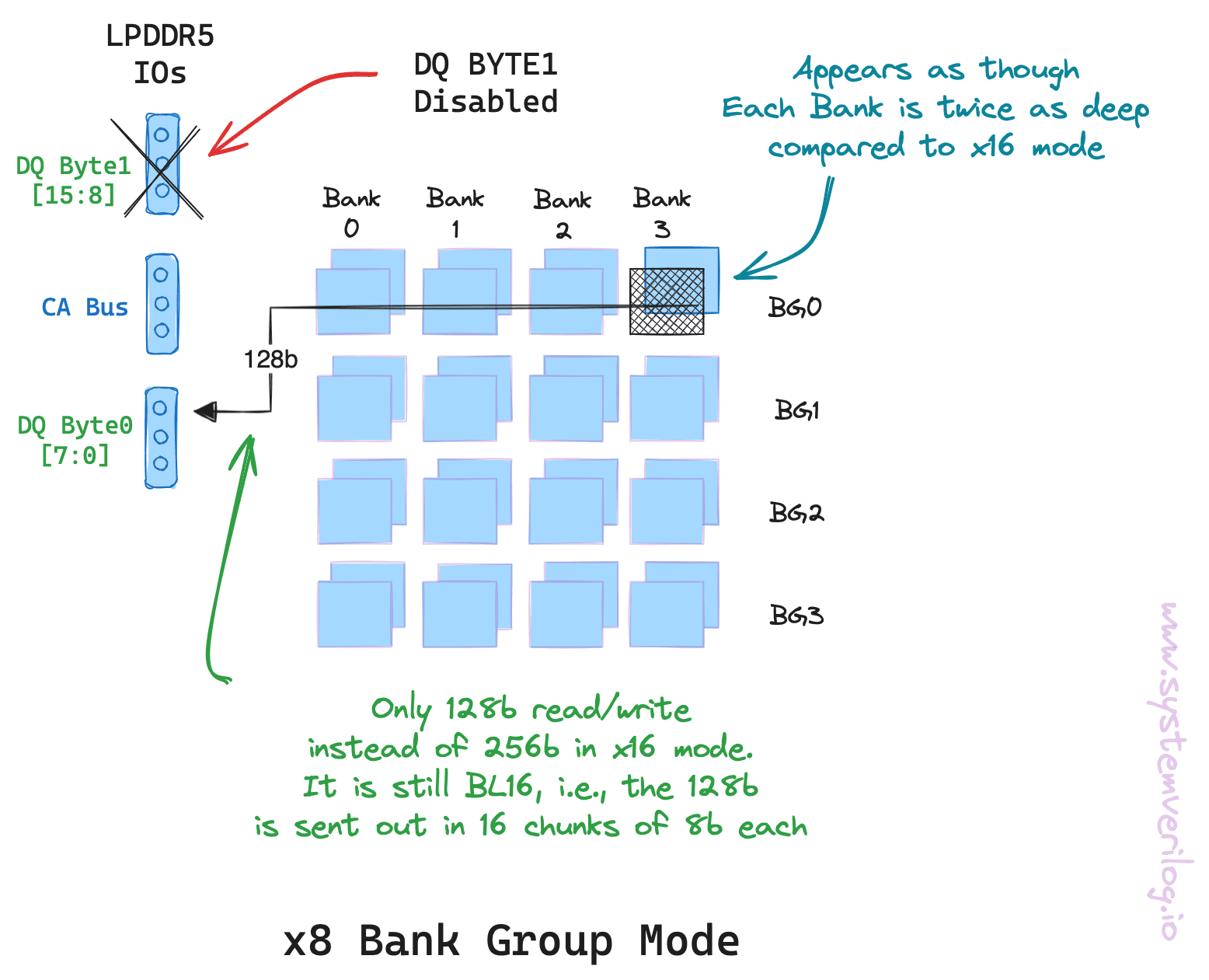
x8 DQ Mode
The LPDDR5 interface has 16 DQ (data) pins. So, by default the memory comes up in what is called x16 DQ mode.
But, you can disable 8 of the DQ pins and put the memory in x8 DQ mode. In this mode only one Bank is activated during a read or write access (instead of 2). In return, what you get is a deeper memory, i.e., each Bank appears to have twice the number of Rows compared to x16 mode. (We cut the access width in half so, as you would expect, the depth doubled.)
| Memory Density | 2Gb | 8Gb | 16Gb | 32Gb |
|---|---|---|---|---|
| Number of Rows | 16,384 | 65,536 | 131,072 | 262,144 |
| Number of Cols | 64 | 64 | 64 | 64 |
| Row Address Bits | R0-R13 | R0-R15 | R0-R16 | R0-R17 |
| Col Address Bits | C0-C5 | C0-C5 | C0-C5 | C0-C5 |
| Bank Address Bits | BA0-BA1 | BA0-BA1 | BA0-BA1 | BA0-BA1 |
| BG Address Bits | BG0-BG1 | BA0-BA1 | BA0-BA1 | BA0-BA1 |
| Page Size | 1KB | 1KB | 1KB | 1KB |
| Array Pre-Fetch | 128b | 128b | 128b | 128b |
in the above table notice how, when compared to Table 1, the Array Pre-Fetch and Page Size halved and Number of Rows doubled.
x16 vs x8 mode is set in mode register MR8.
LPDDR5 Memory Channel
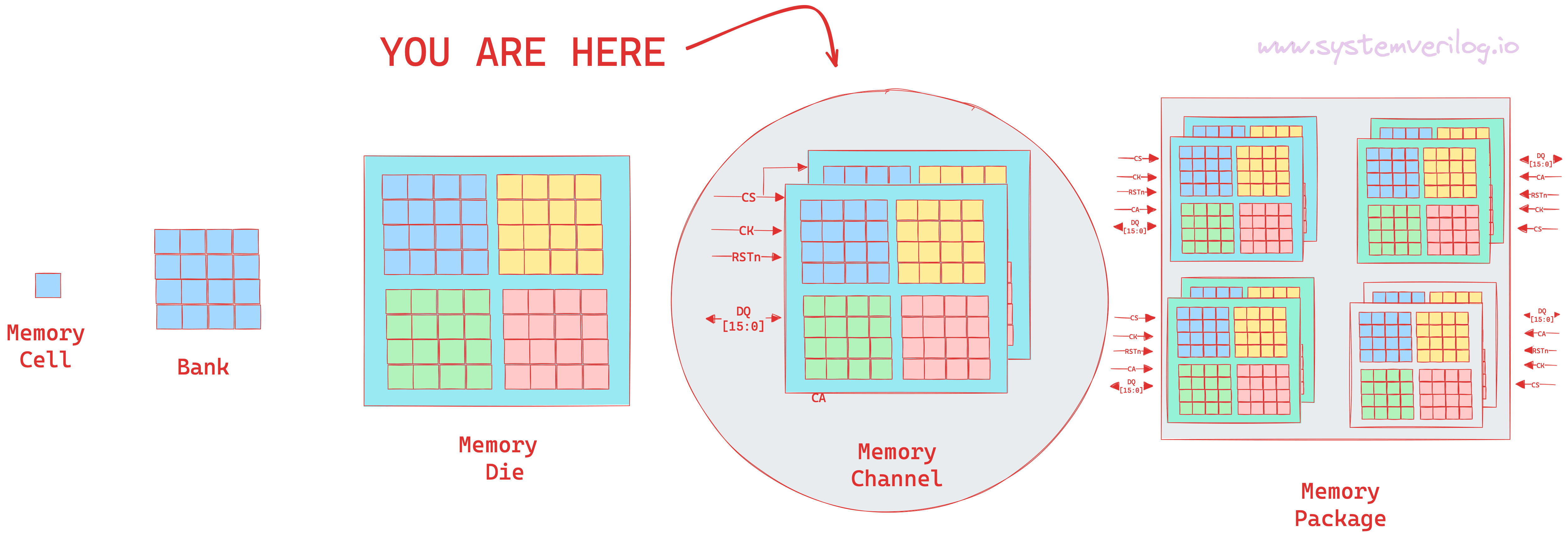
Another common term you will hear in the context of LPDDR5 is "Number of Channels". In the simplest terms, a memory channel is what a LPDDR5 controller interacts with. This interface between a memory controller and a memory channel has the following IOs.
| Pin | Width | Type | Description |
|---|---|---|---|
RESET_n |
1 | Input | Reset pin |
CK_t, CK_c |
1 | Input | Differential clock |
CS[1:0] |
2 | Input | Chip Select. Think of this as the enable/valid pin. The rest of the command bus is valid only when this is high. |
CA[6:0] |
7 | Input | Address bus. This is used to select which BankGroup,Bank,Row,Col to access. |
DQ[15:0] |
16 | InOut | Bidirectional data bus |
WCK[1:0]_t, WCK[1:0]_c |
2 | Input | Differential clocks used for WRITE data capture and READ data output |
DMI[1:0] |
2 | InOut | Data mask inversion. This IO has several functions such as DataMask (DM), DataBusInversion (DBI), or Link ECC based on the mode register setting. |
RDQS[1:0]_t, RDQS[1:0]_c |
1 | RDQS_t: Inout, RDQS_c: Output | Read Data Strobe |
Ranks, Width cascading and depth cascading
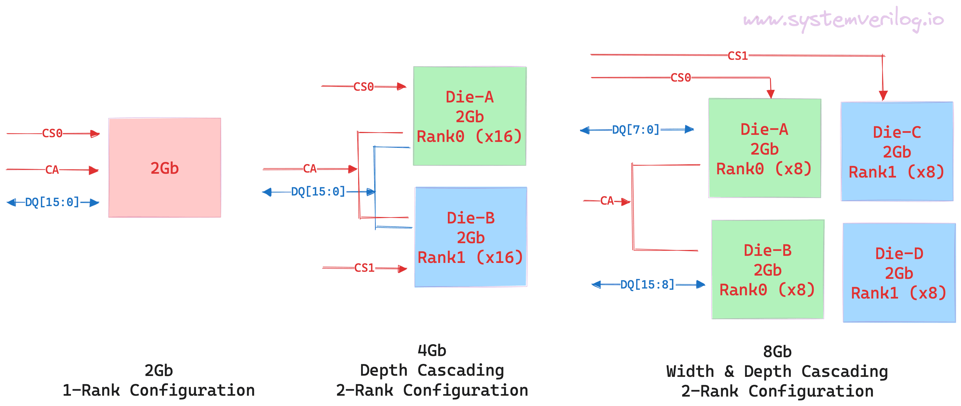
A channel can be composed of one or more LPDDR5 memory dies. In the following figure I've shown how multiple 2Gb memory die can be configured to increase the total memory capacity available in a channel.
- 2Gb Channel Capacity: This is simple. Just a single 2Gb memory die connected to the LPDDR5 IOs.
- 4Gb Channel Capacity: Here, we have 2 x 2Gb dies that are "Depth Cascaded", otherwise called 2-Rank configuration. Die-A is accessed by setting ChipSelect0 (CS0 pin) and Die-B is selected using CS1 pin. But, both dies share the same Address and Data Bus since only one of the ChipSelect pins are active at a time.
- 8Gb Channel Capacity: Here we have 4 x 2Gb dies. Similar to 4Gb capacity, there are 2-Ranks. But within each rank we have 2-dies that are "Width Cascaded", i.e., each of the dies are configured in x8 width mode.
LPDDR5 Memory Package
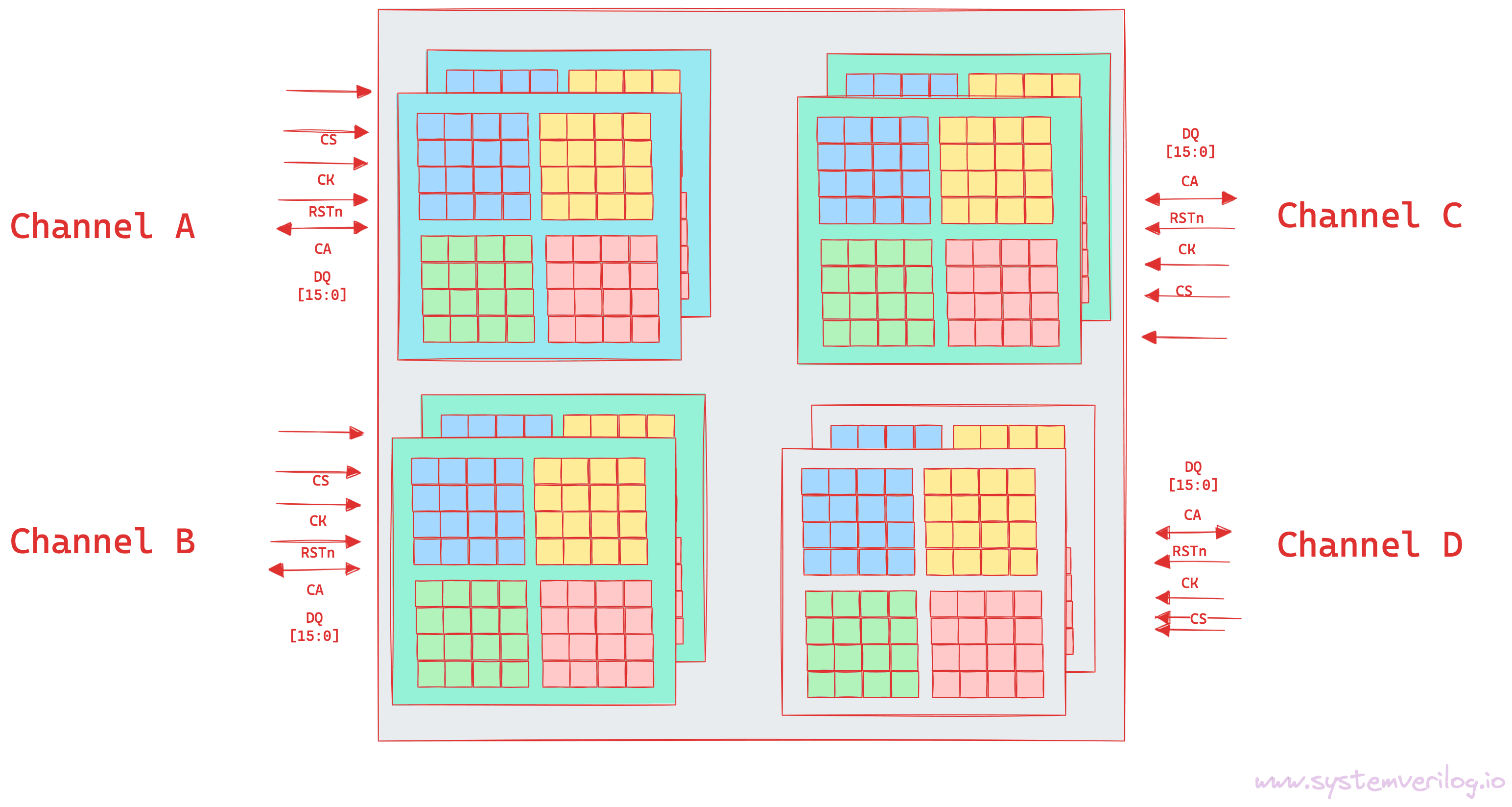
Zoom out one final time and now we have the entire LPDDR5 Memory Device Package. This is what you can purchase from a vendor like Micron or Samsung.
Typically, a memory package holds multiple channels. This allows memory manufacturers to create memory devices with varying Width and Capacity to accommodate various applications.
Typical width and capacities in a vendor's parts catalog are:
- Capacity: 4GB, 8GB, 16GB, etc
- Width: x16 (1-Channel), x32 (2-Channels), x64 (4-Channels). Each channel is independently accessible and have their own set of CA and DQ pins.
The SoC-LPDDR5 Interface
Now that we understand what a LPDDR5 memory looks like, I'll end this article with a discussion on how does a Processor or SoC READ/WRITE to the memory?
In order to communicate with a LPDDR5 memory, an SoC, ASIC, FPGA or Processor requires a Controller and a PHY. Together, these 3 entities - The Controller, The PHY and The LPDDR5 Memory Device form the LPDDR5 memory sub-system.
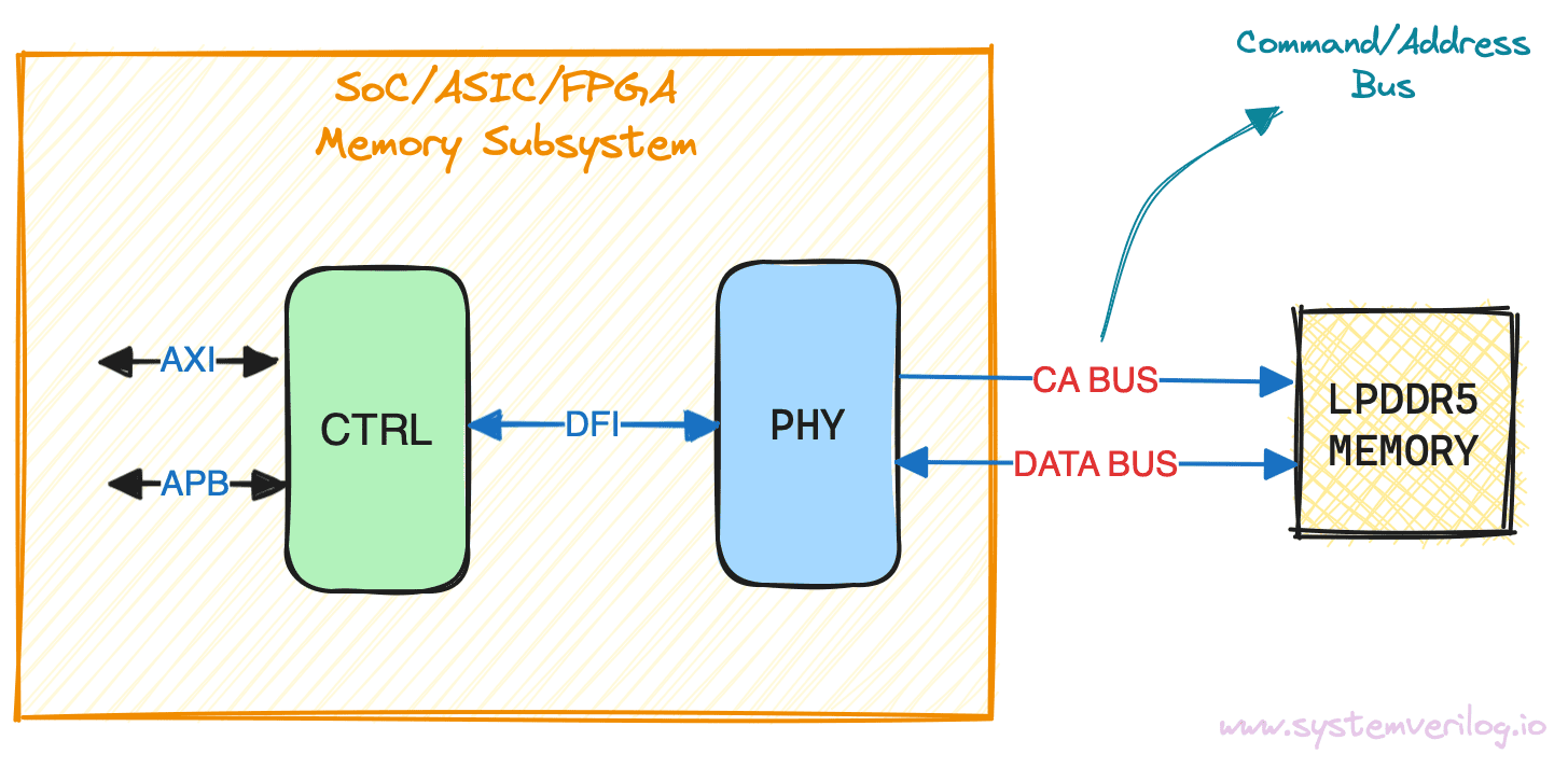
LPDDR5 Interface
As discussed earlier, the following table describes the interface between the PHY and one LPDDR5 memory channel. These IOs are physical traces through the PCB.
| Pin | Width | Type | Description |
|---|---|---|---|
| RESET_n | 1 | Input | Reset pin |
CK_t, CK_c |
1 | Input | Differential clock |
CS |
1 | Input | Chip Select. Think of this as the enable/valid pin. The rest of the command bus is valid only when this is high. |
CA[6:0] |
7 | Input | Address bus. This is used to select which BankGroup,Bank,Row,Col to access. |
DQ[15:0] |
16 | InOut | Bidirectional data bus |
WCK[1:0]_t, WCK[1:0]_c |
2 | Input | Differential clocks used for WRITE data capture and READ data output |
DMI[1:0] |
2 | InOut | Data mask inversion. This IO has several functions such as DataMask (DM), DataBusInversion (DBI), or Link ECC based on the mode register setting. |
RDQS[1:0]_t, RDQS[1:0]_c |
1 | RDQS_t: Inout, RDQS_c: Output | Read Data Strobe |
DFI Interface
You can think of the controller as the logical layer. A large state machine which ensures the LPDDR5 protocol is strictly followed when performing a read, write or refresh operation. The PHY, on the other hand, is the Physical layer. It has all the analog parts required to guarantee the reliable launch and capture of the clock, address and data signals to and from the memory.
Referring to Figure 7 above, the PHY and Controller talk to each other through a well-defined standard interface called the DFI interface. The PHY can communicate to the Controller via this interface whether it is in the initialization phase, calibration phase, or ready to execute a READ/WRITE.
Controller Interface
Accessing a DDR memory is a delicate dance. For example, to WRITE data into the memory, multiple commands need to be issued to the memory to activate the right bank, rows and columns, and a precise time-interval later (called the Write-Latency) the data has to be launched. In between all this, the memory needs to be REFRESHed at a fixed period so that you don't lose any data.
The controller abstracts all of the above complications and presents a simple interface, like AXI, through which you can issue a Write or a Read.
Apart from providing a simple interface to access the memory, the controller also has several smart features (such as address re-ordering) to help the SoC/Processor maximize the memory bandwidth. This is important because the memory is almost always the bottle neck when it comes to performance of your Laptop, Phone or a complex ASIC like the TPUs.
Conclusion
That brings us to the end. In a nutshell, this is what was discussed in this article:
- What exactly is a LPDDR5 memory device made up of.
- What the interfaces to the memory look like.
- How does a Processor or SoC communicate with the memory.
References
- JEDEC JESD-209 LPDDR5 Protocol Specification
- Micron Datasheets
Questions or Comments
Please use this link for any discussions, questions or comments.
If you found this content useful then please consider supporting this site! 🫶