DDR4 SDRAM - Initialization, Training and Calibration
Introduction
When a device with a DRAM sub-system is powered up, a number of things happen before the DRAM gets to an operational state. The following state-machine from the JEDEC specification shows the various states the DRAM transitions through from power-up.
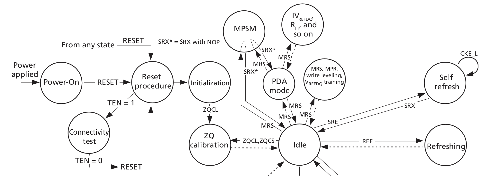
In essence, the initialization procedure consists of 4 distinct phases
- Power-up and Initialization
- ZQ Calibration
- Vref DQ Calibration
- Read/Write Training (a.k.a Memory Training or Initial Calibration)
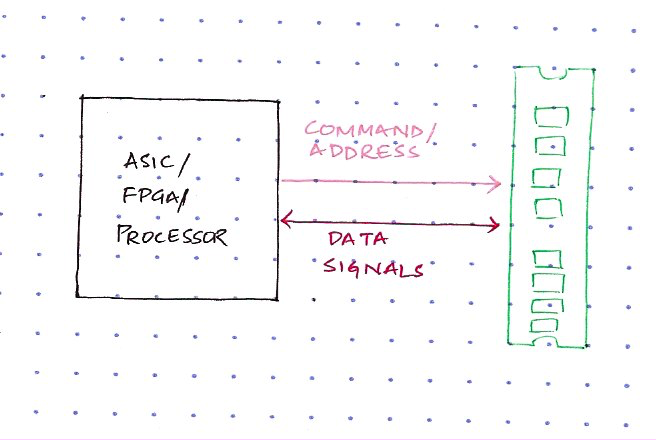
To better understand the following sections, let's assume you have a system which looks like this - An ASIC/FPGA/Processor with 1 DIMM module.
Initialization

Power-up and initialization is a fixed well-defined sequence of steps. Typically, when the system is powered up and the controller in the ASIC/FPGA/Processor is removed out of reset, it automatically performs the power-up and initialization sequence. Here's a super-simplified version of what the controller does. For exact details refer to section 3.3 in the JESD79-49A specification.
- Apply power to the DRAM
- De-assert
RESETand activate ClockEnableCKE - Enable clocks
CK_t/CK_c - Issue
MRScommands and load the Mode Registers [The mode registers are loaded in a specific sequence] - Perform ZQ Calibration [
ZQCL] - Bring the DRAM into
IDLEstate
At this point the DRAMs on the DIMM module understand what frequency they have to operate at, what the CAS Latency (CL), CAS Write Latency (CWL) and few other timing parameters are.
Tip
Check out the article on DDR4 timing parameters to learn more about CL, CWL, etc ...
ZQ Calibration

ZQ Calibration is related to the data pins DQ. To understand what ZQ calibration does and why it is required, we need to first look at the circuit behind each DQ pin. Remember, the DQ pin is bidirectional. It is responsible for sending data back during reads and receiving data during writes.
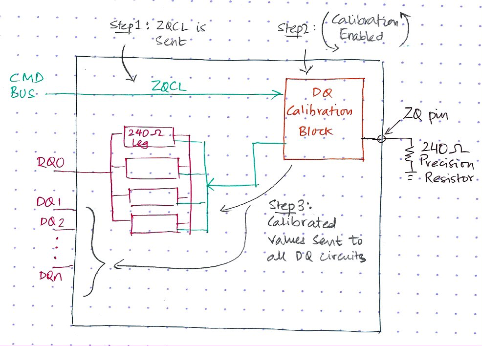
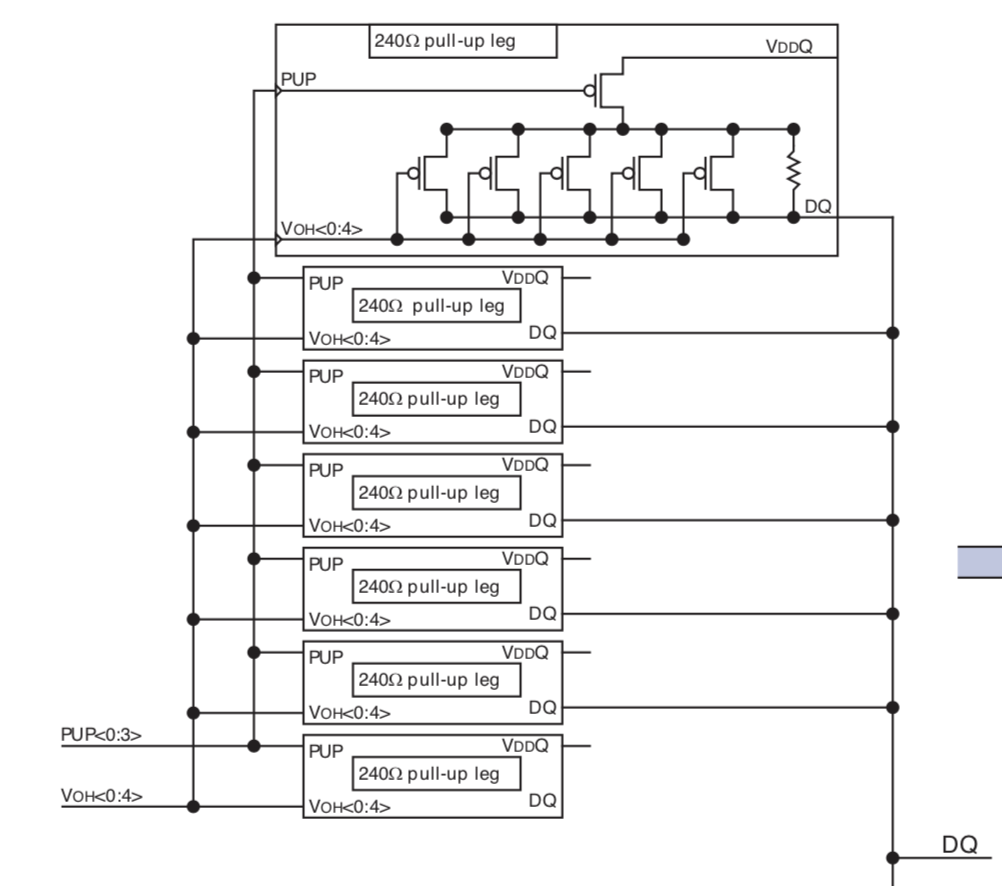
Now, if you look within a DRAM, the circuit behind every DQ pin is made up of a set of parallel 240Ω resistor legs, as shown in Figure 4. Because of the nature of CMOS devices, these resistors are never exactly 240Ω. The resistance is even affected due to voltage and temperature changes. So, they are made tunable.
In order to tune these resistors to exactly 240Ω, each DRAM has
- a special block called DQ calibration control block and
- a ZQ pin to which an external
precision (+/- 1%) 240Ωresistor is connected.
This external precision resistor is the "reference" and it remains at 240Ω at all temperatures. When a ZQCL command is issued during initialization, this DQ calibration control block gets enabled and it produces a tuning value. This value is then copied over to each DQ's internal circuitry.
Note!
The above explanation is a quick overview of ZQ calibration. If you're satisfied, proceed to the next section. If you're itching for more details, read on.
The 240Ω resistor leg within a DQ circuit is a type of resistor called "Poly Silicon Resistor" and is, typically, slightly larger than 240Ω (Poly silicon resistor is a type of resistor that is compatible with CMOS technology). There are number of p-channel devices that are connected in parallel to this poly-resistor so that it can be tuned exactly to 240Ω.
The figure below zooms into one 240Ω leg of the DQ circuit and shows 5 p-channel devices connected to the poly-resistor. These little transistors are set based on input VOH[0:4].
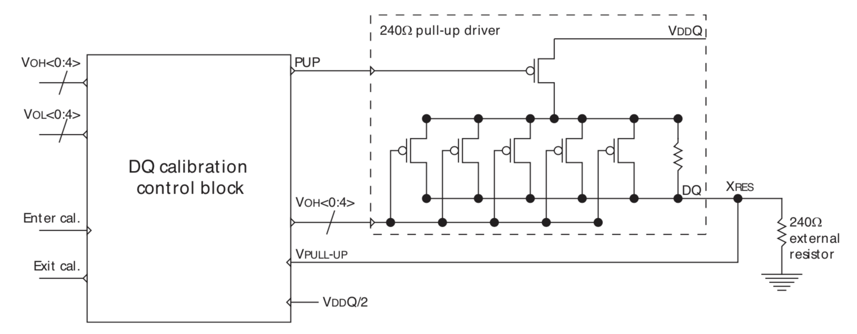
Now, the circuit connected to the DQ calibration control block is essentially a resistor divider circuit with one of the resistors being the poly and the other is the precision 240Ω. When a ZQCL command is issued during initialization, this DQ calibration control block is enabled and an internal comparator within the DQ calibration control block tunes the p-channel devices using VOH[0:4] until the voltage is exactly VDDq/2 (A classic resistor divider). At this point the calibration has been complete and the VOH values are transferred all the DQ pins.
Next, you may wonder why the DQ pins even have this parallel network of 240Ω resistors in the first place!
Having a bank of parallel 240Ω resistors allows you to tune the drive strength (for READs) and termination resistance (for WRITEs). Every PCB layout is different so this tuning capability is required to improve signal integrity, maximize the signal's eye-size and allow the DRAM to operate at high-speeds.
The signal drive strength from the DRAM can be controlled by setting mode register MR1[2:1]. The termination can be controlled using a combination of RTT_NOM, RTT_WR & RTT_PARK in mode registers MR1, 2 & 5 respectively.
Vref DQ Calibration
In DDR4 the termination style of the data lines (DQ) was changed from CTT (Center Tapped Termination, also called SSTL Series-Stud Terminated Logic) to POD (Pseudo Open Drain). This was done to improve signal integrity at high speeds and to save IO power. This is not the first of its kind, GDDR5 (the graphics DRAM) uses POD as well.
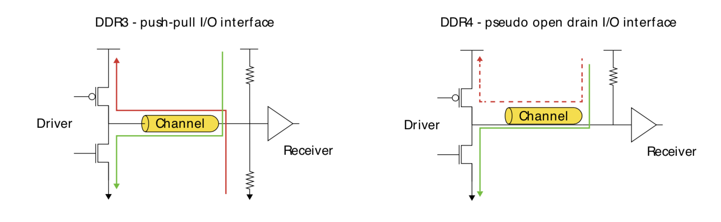
What this means is, in DDR3 Vdd/2 is used as the voltage reference to decide if the DQ signal is 0 or 1. Take another look at the left-hand side of Figure 9, the receiver is essentially a voltage divider circuit.
But in DDR4 there is no voltage divider circuit at the receiver. It instead has an internal voltage reference which it uses to decide if the signal on data lines (DQ) is 0 or 1. This voltage reference is called VrefDQ. The VrefDQ can be set using mode registers MR6 and it needs to be set correctly by the memory controller during the VrefDQ calibration phase.
Read/Write Training
At this point the initialization procedure is complete and the DRAMs are in IDLE state, but the memory is STILL not operational. The Controller and PHY have to perform a few more important steps before data can be reliably written-to or read-from the DRAM. This important phase is called Read/Write Training (or Memory Training or Initial Calibration) wherein the controller (or PHY)
- Runs algorithms to align clock [CK] and data strobe [DQS] at the DRAM
- Runs algorithms and figures out the correct read and write delays to the DRAM
- Centers the data eye for reads
- Reports errors if the signal integrity is bad and data cannot be written or read reliably
This section is about the following circle in the state machine
Why is Read/Write Training Required?
Let's take a closer look at our example system. The picture below shows how the data signals and address/commmand signals are connected between the ASIC/Soc/Processor and the DRAMs on the DIMM.
- The Data and DataStrobe (
DQ & DQS) are connected to each memory in a star topology because each memory is connected to a different portion of the 72 data lines - The Clock, Command & Address lines (
A, CK, CKE, WE, CSn) on a DIMM are connected using a technique called fly-by routing topology. This is done because all DRAMs on the DIMM share the same address lines and fly-by routing is required to achieve better signal integrity and the high speeds.
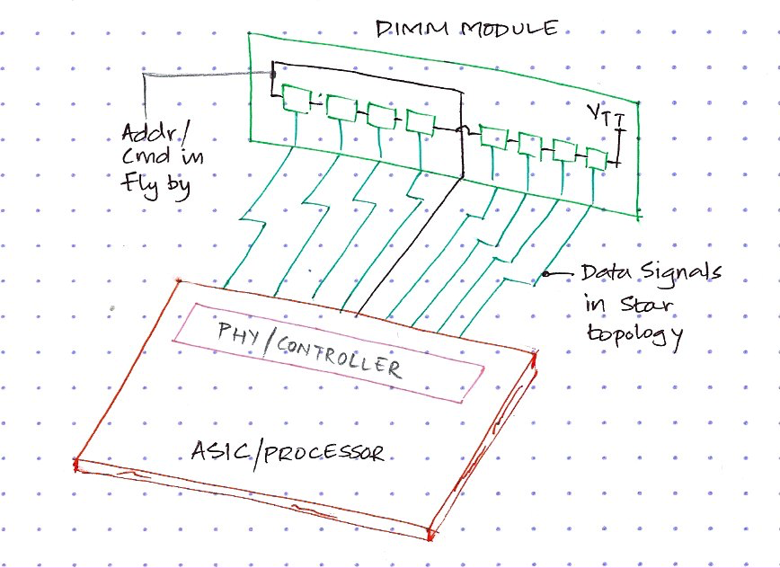
So, from the ASIC/Processor's point of view each DRAM memory on the DIMM is located at a different distance. Or from the DIMM's point of view, the skew between clock and data is different for each DRAM on the DIMM.
The DRAM is a fairly dumb device. Say you intend to do a WRITE operation, during initialization you tell the DRAM what the CAS Write Latency is by programming one of its Mode Registers (CWL is the time delay between the column address and data at the inputs of a DRAM), and you have to honor this timing parameter at all times. The memory controller needs to account for the board trace delays and the fly-by routing delays and launch Address and Data with the correct skew between them so that the Address and Data arrive at the memory with CWL latency between them.
For example, if you program the CAS Write Latency to 9, once the ASIC/uP launches the Column Address, it will need to launch the different data bits at different times so that they all arrive at the DRAMs at a CWL of 9.
Something similar to the above needs to be done for READs as well. Since each DRAM on the DIMM is located at a different distance, when a READ is issued each DRAM on the DIMM will see the READ command at different times and subsequently the data from each DRAM arrives at the ASIC/Processor at different times. During Initial Calibration, the ASIC/Processor figures out what the delays from each of the DRAMs are and trains its internal circuitry accordingly so that it latches the data from the various DRAMs at the right moment.
For Read/Write Training, the Controller/PHY IPs typically offer a number of algorithms. The most common ones are:
Write LevelingMPR (Multi-Purpose Register) Pattern WriteRead CenteringWrite Centering
The following sections go into more detail about each of these algorithms.
Write Leveling
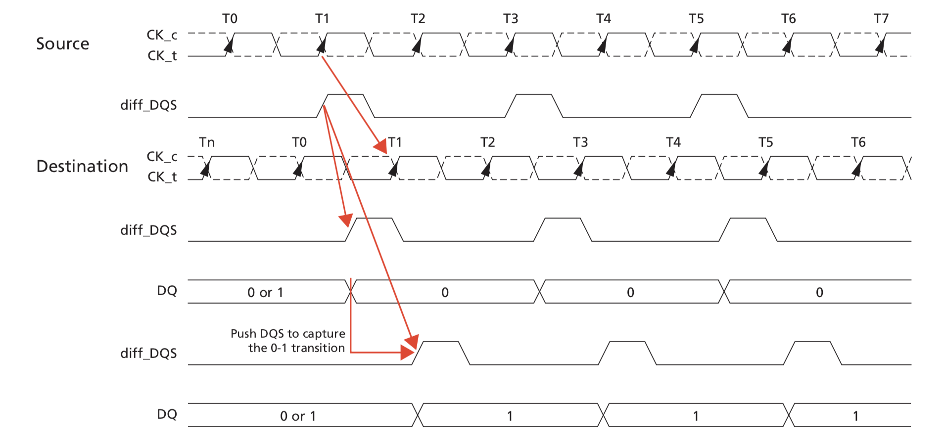
When writing to a DRAM an important timing parameter that cannot be violated is tDQSS. tDQSS is the position of the DataStrobe (DQS) relative to Clock (CK). tDQSS has to be within a tDQSS(MIN) and tDQSS(MAX) as defined in the spec. If tDQSS is violated and falls outside the range, wrong data may be written to the memory.
Since the Clock to Data/DataStrobe skew is different for each DRAM on the DIMM, the memory controller needs to train itself so that it can compensate for this skew and maintain tDQSS at the input of each DRAM on the DIMM.
When you enable write-leveling in the controller, it does the following steps:
- Does an Mode Register write to MR1 to set bit 7 to 1. This puts the DRAM into write-leveling mode. In write-leveling mode, when the DRAM sees a DataStrobe (DQS), it uses it to sample the Clock (CK) and return the sampled value back to the controller through the DQ bus.
- The controller then sends a series of DQS pulses. Since the DRAM is in write-leveling mode, it samples the value of CK using DQS and returns this sampled value (either a 1 or 0), back to the controller, through the DQ bus.
- The controller then
- looks at the value of the DQ bit that is returned by the DRAM
- either increments or decrements the DQS delay and
- launches the next set of DQS pulses after some time
- The DRAM once again samples CK and returns the sampled value through DQ bus
- Steps 2 to 4 are repeated until the controller sees a 0-to-1 transition. At this point the controller locks the DQS delay setting and write-leveling is achieved for this DRAM device.
- Steps 2 to 5 are then repeated for each DQS for the whole DIMM to complete the write-leveling procedure
- The DRAMs are finally removed out of write-leveling mode by writing a 0 to MR1[7]
The figure below shows the write-leveling concept.
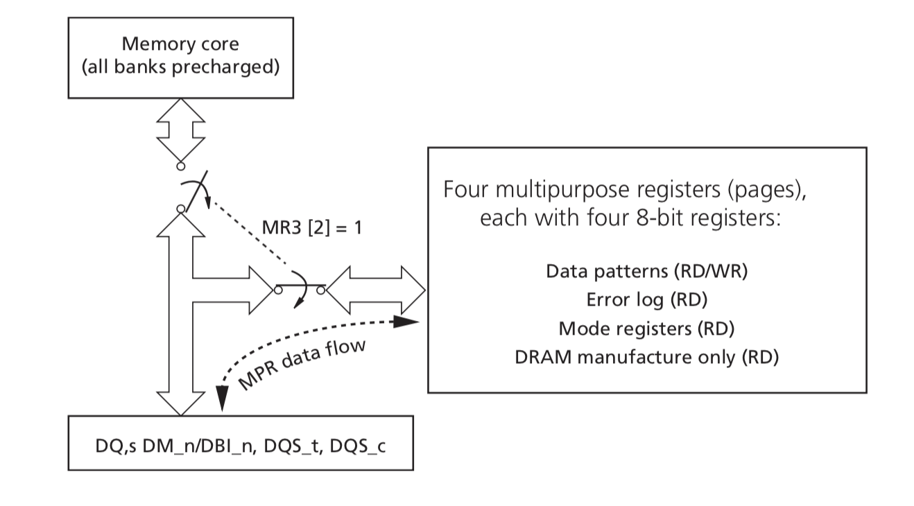
MPR Pattern Write
MPR (Multi Purpose Register) Pattern Write isn't exactly a calibration algorithm. It is typically a step that is performed before Read Centering and Write Centering.
DDR4 DRAMs contain four 8-bit programmable registers called MPR registers that are used for DQ bit training (i.e., Read and Write Centering). MPR access mode is enabled by setting Mode Register MR3[2] = 1. When this mode is enabled READs and WRITEs issued to the DRAM are diverted to the Multi Purpose Register instead of the memory banks.
Read Centering
The purpose of read centering is to train the internal read capture circuitry in the controller (or PHY) to capture the data in the center of the data eye. The memory controller (or PHY)
- Enables bit 2 in mode register MR3 so that the DRAM returns data from the Multi Purpose Register (MPR) instead if the DRAM memory.
- Then initiates a continuous stream of READs. The memory returns the pattern that was written in the previous MPR Pattern Write step. Let's assume this pattern is an alternating
1-0-1-0-... - While the READs are going on, the internal read capture circuitry either increases of decreases an internal read delay register to find the left and right edge of the data eye.
- When the edges of the eye are detected, the read delay registers are set appropriately to ensure the data is captured at the eye center.
- The above steps are repeated for each of the DQ data bits
Write Centering
Similar to the read centering step, the purpose of write centering is to set the write delay for each data bit so that write data is centered on the corresponding write strobe edge at the DRAM device.
During write centering the PHY does the following WRITE-READ-SHIFT-COMPARE loop continuously
- Initiates a continuous stream of WRITEs and READs
- Incrementally changes write delay of the data bits
- Compares the data read back to the data written
From the above loop the PHY can determine for what write-delay range it reads back good data, and hence it can figure out the left and write edges of the write-data eye. Using this dat,a the DQ is centered to the DQS for writes.
Periodic Calibration
In a device such as a network switch or router, there could be changes in Voltage and Temperature during its course of operation. To keep the signal integrity and data access reliable, some of the parameters that were trained during initialization and read/write training have to be re-run. Memory controller and PHY IPs typically provide the following two periodic calibration processes.
Periodic ZQ- Also known as ZQ Calibration Short (ZQCS). It is used to run ZQ calibration periodically to tune the 240Ω resistor that was described earlier.Periodic Read Centering- To re-calculate read delays and other read related parameters
Enabling periodic calibration is optional because if you know your device will be deployed in stable temperature conditions, then the initial ZQ calibration and read/write training is sufficient.
Typically, the memory controller or PHY allow you to set a timer and enable periodic calibration through their registers. Once the timer is set, periodic calibration is run every time the timer expires.
In a Nutshell
There are 4 steps to be completed before the DRAM can be used
- Power-up and initialization
- ZQ Calibration
- Vref DQ Calibration
- Read/Write Training
Once this is done system is officially in IDLE and operational. You may need to enable periodic calibration depending upon the conditions in which your device is deployed.
Reference
- JEDEC specification
- A number of Micron DDR4 Datasheets
- A number of Micron DDR3 Datasheets
- Rambus - Fly-By Topology
- AIC Design - Resistors and Inductors
- Bit-Tech
- EETimes
- JEDEC DDR4 Mini Workshop
- Cadence
- Texas Instruments
Questions & Comments
For questions or comments on this article, please use the following link.
If you found this content useful then please consider supporting this site! 🫶