DDR4 Tutorial - Understanding the Basics
Introduction
DDR4 SDRAMs are very prevalent in devices that use ASICs and FPGAs. In this article we explore the basics.
- What a DDR4 SDRAM looks like on the inside
- What goes on during basic operations such as READ & WRITE, and
- A high-level picture of the SDRAM sub-system, i.e., what your ASIC/FPGA needs in order to talk to a DDR4 SDRAM memory
Physical Structure
A good place to start is to look at some of the essential IOs and understand what their functions are. From there we'll dive deeper until we get to the basic unit that makes up a DRAM memory.
Top Level
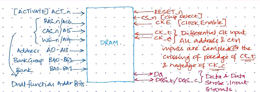
As you would expect, the DRAM has clock, reset, chip-select, address and data inputs. The table below has little more detail about each of them. This is not a complete list of IOs, only the basic ones are listed here. Take a little time to carefully read what each IO does, especially the dual-function address inputs.
| Symbol | Type | Function |
|---|---|---|
| RESET_n | Input | DRAM is active only when this signal is HIGH |
| CS_n | Input | The memory looks at all the other inputs only if this is LOW. |
| CKE | Input | Clock Enable. HIGH activates internal clock signals and device input buffers and output drivers. |
| CK_t/CK_c | Input | Differential clock inputs. All address & control signals are sampled at the crossing of posedge of CK_t & negedge of CK_n. |
| DQ/DQS | Inout | Data Bus & Data Strobe. This is how data is written in and read out. The strobe is essentially a data valid flag. |
| RAS_n/A16 CAS_n/A15 WE_n/A14 | Input | These are dual function inputs. When ACT_n & CS_n are LOW, these are interpreted as Row Address Bits. When ACT_n is HIGH, these are interpreted as command pins to indicate READ, WRITE or other commands. |
| ACT_n | Input | Activate command input |
| BG0-1 BA0-1 | Input | Bank Group, Bank Address |
| A0-13 | Input | Address inputs |
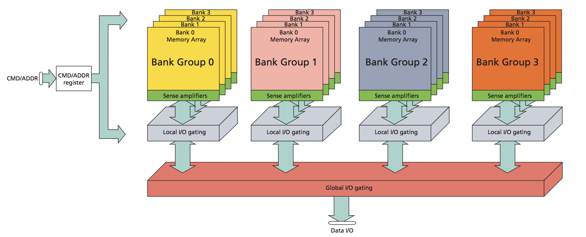
Bank Group, Bank, Row, Column
The top-level picture shows what a DRAM looks like on the outside. Going a level deeper, this is how memory is organized - in Bank Groups and Banks.
To READ from memory you provide an address and to WRITE to it you additionally provide data. This address provided by you, the user, is typically called "logical address". This logical address is translated to a physical address before it is presented to the DRAM. The physical address is made up of the following fields:
- Bank Group
- Bank
- Row
- Column
these individual fields are then used to identify the exact location in the memory to read-from or write-to.
Going down another level, this is what you'll see within each Bank.
- Memory Arrays
- Row Decoder
- Column Decoder
- Sense Amplifiers
Once the Bank Group and Bank have been identified, the Row part of the address activates a line in the memory array. This is called the "Word Line" and activating it reads data from the memory array into something called "Sense Amplifiers". The Column address then reads out a part of the word that was loaded into the Sense Amps. The width of the column is called the "Bit Line".
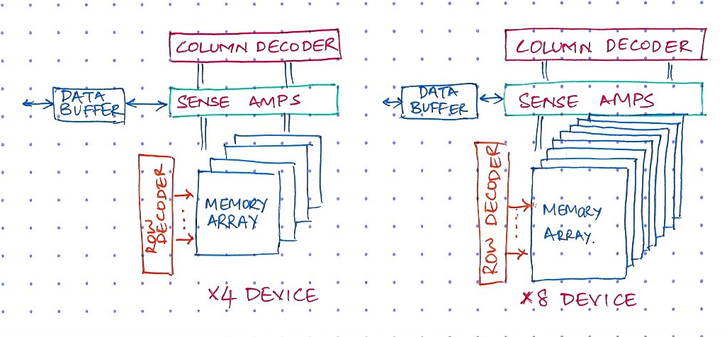
The width of a colum is standard - it is either 4 bits, 8 bits or 16 bits wide and DRAMs are classified as x4, x8 or x16 based on this column width. Another thing to note is that, the width of DQ data bus is same as the column width. So, to simplify things, you can say that DRAMs are classified based on the width of the DQ bus. More in this below.
Note
x16 devices have only 2 Bank Groups whereas x4 and x8 have 4 as shown in figure 2.
Tip
Analogy Time
A DRAM chip is equivalent to a building full of file cabinets
Bank GroupIdentifies the floor number
Bank AddressIdentifies the file cabinet within that floor where the file you need is located
Row AddressIdentifies which drawer in the cabinet the file is located. Reading data into the Sense Amplifiers is equivalent to opening/pulling out the file drawer.
Col AddressIdentifies the file number within this drawer
At the lowest level, a bit is essentially a capacitor that holds the charge and a transistor acting as a switch.
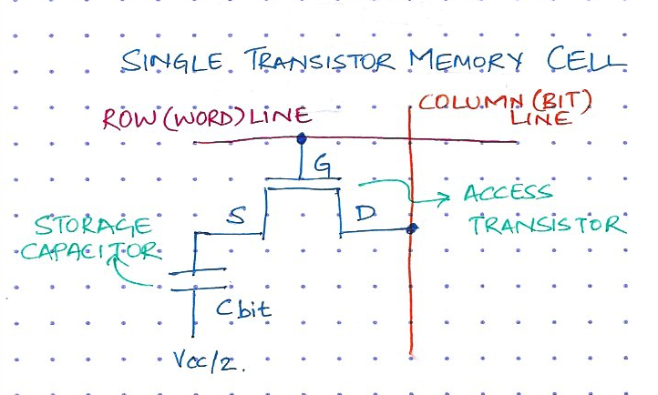
Since the capacitor discharges over time, the information eventually fades unless the capacitor is periodically REFRESHed. This is where the 'D' in DRAM comes from - it refers to Dynamic as opposed to SRAM (Static Random Access Memory).
DRAM Sizing & Addressing
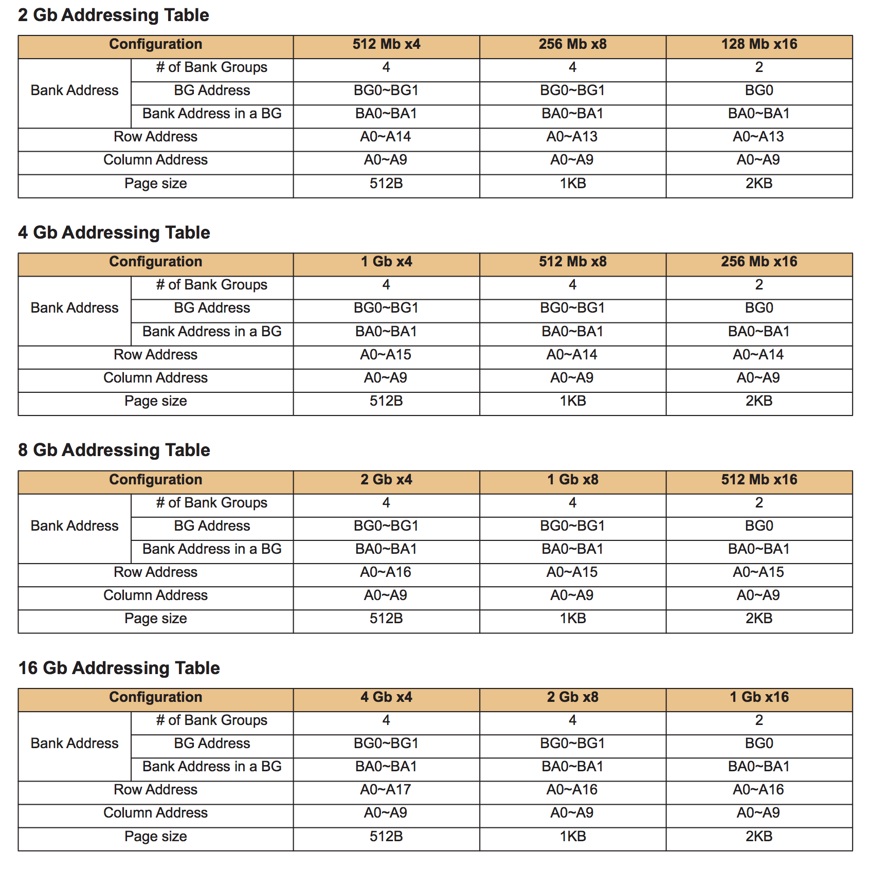
DRAMs come in standard sizes and this is specified in the JEDEC spec. JEDEC is the standards committee that decides the design and roadmap of DDR memories. The following figure is from section 2.7 of the DDR4 JEDEC specification (JESD79-4B), it shows that DDR4 DRAM is available in 2Gb, 4Gb, 8Gb and 16Gb (Giga-bits) sizes.
Row Address
Depending on the size of the DRAM the number of ROW and COLUMN bits change. I think this is self-explanatory, 8Gb (x4) has more addressable memory than 2Gb (x4), so the 8Gb has 17 ROW address bits (A0 to A16) whereas 2Gb has only 15 (A0 to A14).
Column Address
Regardless of the size of the DRAM, it always has only 10 column bits A0 to A9. This means there are only 2^10 = 1K columns.
DRAM Width
DDR4 DRAMs are available in 3 widths x4, x8 and x16. This indicates the number of data pins (DQ) on the DRAM.
x4has 4 data pinsDQ[3:0]x8has 8 data pinsDQ[7:0]x16has 16 data pinsDQ[15:0].
When you READ an address from a DDR4 DRAM the data is returned as a burst of 8 (typically called the Burst Length 8 or BL8 mode). Figure 8 shows what this looks like. In a x4 DRAM the memory returns 32-bits of data with every READ operation (8 burts of data is returned with 4 bits in each burst), in case of x8 64 bits is returned and in case x16 devices 128 bits (BL8 x 16).
Tip
This concept of DRAM Width is very important, so let me explain it once more a little differently.
Going back to my analogy, I said:
ROWaddress identifies which drawer in the cabinet the file is located, andCOLUMNaddress identifies where in the drawer the file is located.
Now, extending this analogy a bit more -- DDR4 DRAM is offered in 4 "file cabinet sizes": 2Gb (extra-small cabinet), 4Gb (medium), 8Gb (large) and 16Gb(extra-large)).
Now, apart from the 4 file cabinet sizes -- if you consider each cabinet, say, the 4Gb medium size cabinet, it is offered in 3 form factors based on the size of paper it can hold. So, you can buy a 4Gb cabinet which can hold A5 size paper(x4) or A4 size paper (x8) or A3 size paper (x16).
DRAM Page Size
In the Figure 5 table, there's a mention of Page Size. Continuing from the last section on DRAM Width, this concept is easy to understand -- The x4 cabinet holds A5 size pages (small page size - 512B); x8 cabinet holds A4 size pages (medium page size - 1KB); x16 cabinet holds A3 size pages (large page size - 2KB).
Here's another explanation which is more accurate and technical --
Reading from DRAM memory is a 2-step process (More on this in a following section) Page size is essentially the number of bits per row. Or put it another way, it is the number of bits loaded into the Sense Amps when a row is activated. Since the column address is 10 bits wide, there are 1K bit-lines per row. So, for a x4 device number of bits is 1K x 4 = 4K bits (or 512B). Similarly, for x8 device it is 1KB and for x16 it is 2KB per page.
DRAM Size Calculation
Let's try to make some more sense of the above table by hand-calculating two of the sizes
/* 4Gb x4 Device */
Number of Row Address bits: A0-A15 = 16 bits
    Total number of rows = 2^16 = 64K
Number of Column Address bits: A0-A9 = 10 bits
    Number of columns per row = 1K
Width of each column = 4 bits
Number of Bank Groups = 4
Number of Banks = 4

Total DRAM Capacity =
    Num.Rows x
    Num.Columns x Width.of.Column x
    Num.BankGroups x Num.Banks

Total DRAM Capacity =
    64K x 1K x 4 x 4 x 4 = 4Gb

/* 4Gb x8 Device */
Number of Row Address bits: A0-A14 = 15 bits
    Total number of rows = 2^15 = 32K
Number of Column Address bits: A0-A9 = 10 bits
    Number of columns per row = 1K
Width of each column = 8 bits
Number of Bank Groups = 4
Number of Banks = 4

Total DRAM Capacity =
    Num.Rows x
    Num.Columns x Width.of.Column x
    Num.BankGroups x Num.Banks

Total DRAM Capacity =
    32K x 1K x 8 x 4 x 4 = 4Gb
Rank (Depth Cascading)
When dealing with DRAMs you'll come across terminology such as Single-Rank, Dual-Rank or Quad-Rank. Rank is the highest logical unit and is typically used to increase the memory capacity of your system.
Say you need 16Gb of memory. Depending on what's available in the market and what is cheaper, you could have a single 16Gb memory die, in this case you would call it a Single Rank system because you just need 1 ChipSelect signal (CS_n) to read all the contents of the memory. Or you could choose to have 2 individual 8Gb discrete devices soldered down on the PCB (because 2x8Gb devices happen to be cheaper than 1x16Gb). In this case the 2 devices will be connected to the same address and data busses, but you will need 2 ChipSelects to separately address each device. Since you need two ChipSelects, this setup is called Dual-Rank.
Note
One other DRAM variety you may come across is a "Dual-Die Package" or DDP. In this case you'll have a single DRAM chip soldered on the board but internally within the package it'll have a stack of 2 dies. Each die will once again share address and data lines but will have separate chip selects, making it a Dual Rank device.
![]()
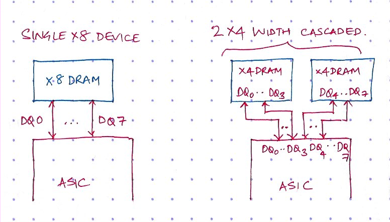
Width Cascading
Another example - Say you need an 8Gb memory and the interface to your chip is x8. Then you could pick a single 8Gb x8 device or two 4Gb x4 devices and connect them in a "width cascaded" fashion on the PCB. With width cascading, both DRAMs are connected to the same ChipSelects, Address and Command bus, but use different portions of the data bus (DQ & DQS). In the picture below, the first x4 DRAM is connected to DQ[3:0] and the second on to DQ[7:4].
Accessing Memory
- Read and write operations to the DDR4 SDRAM are burst oriented. It starts at a selected location (as specified by the user provided address), and continues for a burst length of eight or a ‘chopped’ burst of four.
- Read and write operations are a 2-step process. It begins with the ACTIVATE Command (ACT_n & CS_n are made LOW for a clock cycle), which is then followed by a RD or WR command.
- The address bits registered coincident with the ACTIVATE Command are used to select the BankGroup, Bank and Row to be activated (BG0-BG1 in x4/8 and BG0 in x16 selects the bankgroup; BA0-BA1 select the bank; A0-A17 select the row). This step is also called RAS - Row Address Strobe.
- The address bits registered coincident with the Read or Write command are used to select the starting column location for the burst operation. This step is also referred to as CAS - Column Address Strobe.
- Each bank has only one set of Sense Amps. Before a read/write to a different row in the same bank can be performed, the current open row has to be de-activated using a PRECHARGE command. PRECHARGE is equivalent to closing the current file drawer in the cabinet, it causes the data in the Sense Amps to be written back into the row.
- Instead of issuing an explicit PRECHARGE command to deactivate a row, the RDA (Read with Auto-Precharge) and WRA (Write with Auto-Precharge) commands can be used. These commands tell the DRAM to automatically deactivate/precharge the row once the read or write operation is complete. Since column address uses only address bits A0-A9, A10 which is an unused bit during CAS is overloaded to indicate Auto-Precharge.
Command Truth Table
I'm constantly referring to something called "commands" - ACTIVATE command, PRECHARGE command, READ command, WRITE command. But in the very first picture of this article, there is no "Command" input to the DRAM. So how are these commands issued?
Well, the DRAM interprets the ACT_n, RAS_n, CAS_n & WE_n inputs as commands based on the truth table below.
| Function | Shortcode | CS_n | ACT_n | RAS_n/A16 | CAS_n/A15 | WE_n/A14 | A10/AP |
|---|---|---|---|---|---|---|---|
| Refresh | REF | L | H | L | L | H | H or L |
| Single Bank Precharge | PRE | L | H | L | H | L | L |
| Bank Activate | ACT | L | L | Row Address | |||
| Write | WR | L | H | H | L | L | L |
| Write with Auto-Precharge | WRA | L | H | H | L | L | H |
| Read | RD | L | H | H | L | H | L |
| Read with Auto-Precharge | RDA | L | H | H | L | H | H |
The table above is only a subset of commands you can issue to the DRAM. The entire DDR4 command truth table is specified in section 4.1 of the JEDEC spec JESD79-4B.
Read
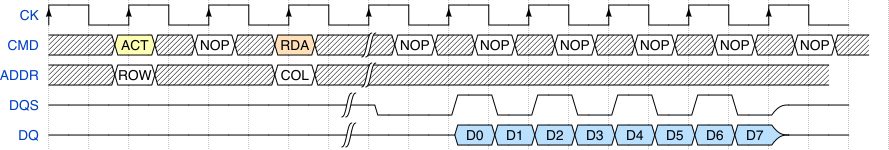
Figure 8 shows the timing diagram of a READ operation with burst length of 8 (BL8).
- The first step is an
ACTcommand. The value on the address bus at this time indicates the row address. - In the second step a
RDA(Read with Auto-Precharge) is issued. The value on the address bus during at this time is the column address. - The RDA command tells the DRAM to automatically
PRECHARGEsthe bank after the read is complete
Write
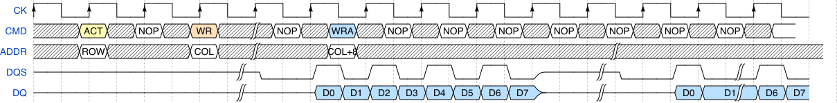
Figure 9 shows the timing diagram of a WRITE operation.
- The first step activates a row
- Then 2
WRITEcommands are issued. The first one to addressCOLand second one toCOL+8. - The second write operation does not need an
ACTbefore it because the row we intend to write to is already active in the Sense Amps - Also note that the first command is a plain
WR, so this leaves the row active. The second command is aWRAwhich de-activates the row after the write completes.
Note
I sneaked something in here without much explanation. A16, A15 & A14 are not the only address bits with dual function. The auto precharge command is issued via A10, and select BurstChop4 (BC4) or BurstLength8 (BL8) mode is selected via A12, if enabled in the mode register.
DRAM sub-system
Now that we've had a sufficiently long discussion about the DRAM, it is time to talk about what the ASIC or FPGA needs in-order to talk to the DRAM. This is called the DRAM sub-system and it's made up of 3 components:
- The DRAM memory itself, which comprises of everything described above
- A DDR PHY
- A DDR Controller
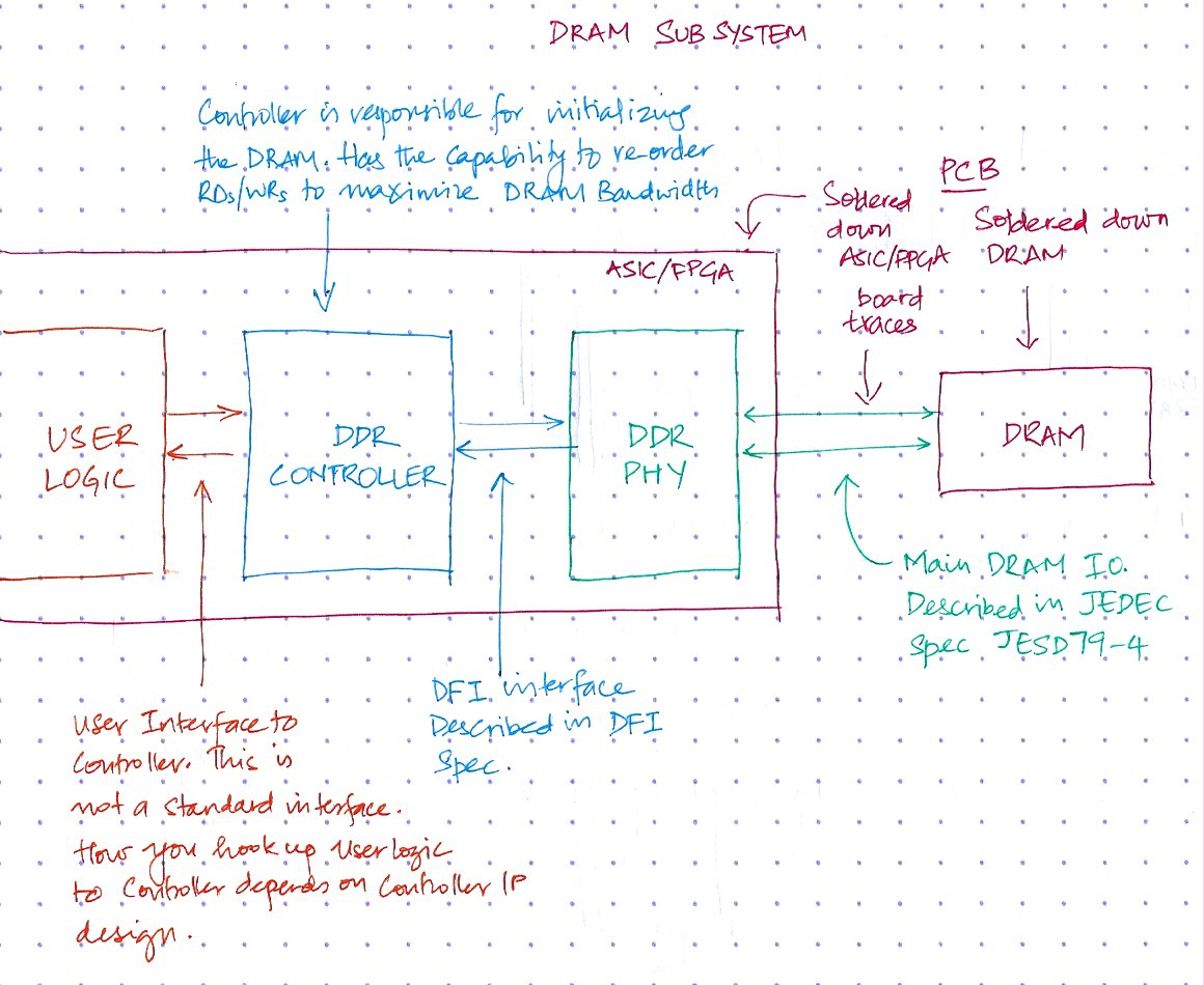
There's a lot going on in the picture above, so lets break it down:
- The DRAM is soldered down on the board. The PHY and controller, along with user logic are typically part of the same FPGA or ASIC.
- The interface between the user-logic and the controller can be user defined and need not be standard
- When the user-logic makes a read or write request to the controller, it issues a logical address
- The controller then converts this logical address to a physical address and issues a command to the PHY
- The Controller and PHY talk to each other over a standard interface called the DFI interface. You can download the DFI specification from here.
- The PHY then does all the lower level signaling and drives the physical interface to the DRAM.
- This interface between the PHY and memory is specified in the JEDEC standard JESD79-49B specification
Think of the controller as the brains and the PHY as the brawns.
- When you activate a row, the whole page is loaded into the Sense Amps, so multiple reads to an already open page are lesser expensive because you can skip the first step of row activation. The controller typically has the capability to re-order requests issued by the user to take advantage of this. To do the re-ordering it uses a small cache or TCAM and always returns the latest data, so you don't have to worry about stale data or collisions occurring because of this re-ordering done by the controller.
- The PHY contains the analog drivers and provides the capability to tweak registers to increase drive strength or change terminations, in order to improve signal integrity.
In a Nutshell
Let's wrap this up
- The DRAM is organized as Bank Groups, Bank, Row & Columns
- The address issued by the user is called Logical Address and it is converted to a Physical Address by the DRAM controller, before it presented to the memory
DDR4 DRAMs are classified as
x4, x8 or x16based on the width of theDQdata bus - You can depth cascade or width cascade DRAMs to achieve the required size
- Read and write operations are a 2-step process. 1st step activates a row, 2nd step reads or write to the memory.
- The DRAM sub system comprises of the memory, a PHY layer and a controller
Questions & Comments
For questions or comments on this article, please use the following link.
If you found this content useful then please consider supporting this site! 🫶